

The Solar Energy Research Institute of Singapore (SERIS) at NUS is embarking on a series of research projects over the next 10 years to strengthen and deepen its solar capabilities.
Three flagship R&D projects
(1) Perovskite-silicon tandem solar cells and modules
Prof Armin ABERLE (Project Leader), Assoc Prof Erik BIRGERSSON, Asst Prof HOU Yi, Dr Firdaus BIN SUHAIMI, Dr CHOI Kwan Bum, Dr JANG Yu Jin, Dr KIM Jinhyun, Dr LUO Chao, Dr Romika SHARMA, Dr WANG Puqun, Mohd Asri BIN MOHD HAMDAN, Gabby Alonzo DE LUNA, Elisaveta UNGUR PhD students: Varsha DAHIYA, DU Xinyi, Stella HADIWIDJAJA, LEE Ling Kai, Erik SPAANS, YAP Qi Jia, ZHOU Qilin
Introduction
Singapore’s space constraints necessitate the installation of solar PV systems with very high efficiencies to maximise PV power generation. While single-junction crystalline silicon (Si) solar cells have a theoretical efficiency limit of about 30% under the standard 1-Sun solar spectrum (AM1.5G), stacking a second solar cell with a larger electronic bandgap onto a silicon cell to create a two-junction (or “tandem”) solar cell offers the potential for much higher power conversion efficiencies while maintaining low manufacturing costs ($/W). For 2-junction Si-based tandem solar cells the theoretical 1-Sun efficiency limit is about 44%, whereby a practical cell efficiency limit of around 35% seems possible in future mass production (beyond 2030). Due to this excellent PV efficiency potential, Si-based tandem solar cells are of very high importance to Singapore’s solar sector, for both manufacturing and deployment. This flagship project focuses on exploring low-cost wide-bandgap thin-film materials, in particular
metal halide perovskites, as the absorber layer of the top cell on a silicon bottom cell. In 2025 our research efforts focused on the improvement of perovskite-Si tandem cells with small (1 cm²), medium (16 cm²) and large (244 cm²) areas, the improvement of the efficiencies of our 1-cell mini-modules with active areas of up to 244 cm², and outdoor monitoring of encapsulated tandem mini-modules to study their long-term reliability in Singapore’s tropical climate.
Small (1 cm²) perovskite-Si tandem solar cells on textured Si bottom cells
In 2025, SERIS’ Perovskite-based Multijunction Solar Cells Group achieved 33.3% efficiency for a perovskite-silicon tandem solar cell using an industrially fabricated Cz heterojunction silicon bottom cell with cell area of 1 cm², see Fig. 1. The measurement was performed at SERIS. This was accomplished by successfully forming high-quality 1.66-eV perovskite films on textured silicon surfaces using the spin-coating method. A key challenge in this work was improving the perovskite crystal quality on silicon architectures. We introduced a ligand that effectively controls the principal organic cations to regulate crystallisation. Our organic control approach supplements previous strategies mainly focused on strong coordination with inorganic lead halides, enabling refined crystal growth and improved film quality of perovskite films on thin Si wafers. We effectively minimised the quality gap between perovskite films grown on glass and those grown on thin Si substrates, thereby enabling high-quality wide-bandgap perovskite films being integrated with industrially fabricated Cz silicon bottom cells. The group’s ongoing efforts are focused on closing the gap to the current world-record 1cm² perovskite-silicon tandem solar cell (34.8%, LONGi, China).
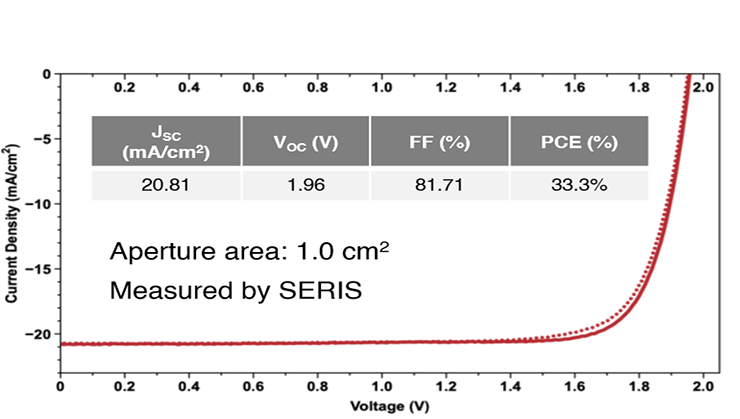
Fig. 1: Measured J-V curves of a 33.3% efficient perovskitesilicon tandem solar cell (1.0 cm2 aperture area) made at SERIS using a Cz heterojunction silicon bottom cell. The silicon cell has pyramid-textured front and rear surfaces. The perovskite absorber was made by spin coating.
Upscaling of perovskite-silicon tandem solar cells to medium and large areas (16 and 244 cm²)
In 2025, SERIS’ NISCM Cluster continued to make good progress with improving the PV efficiencies of perovskite-silicon tandem solar cells with active areas of 16 and 244 cm², as shown in the photographs of Fig. 2. Both the silicon bottom cells (heterojunction, Cz wafers) and the perovskite top cells were fully made in SERIS. A low-temperature screen-printed silver metallisation was utilised on both sides of the 2-terminal (2T) tandem solar cells.
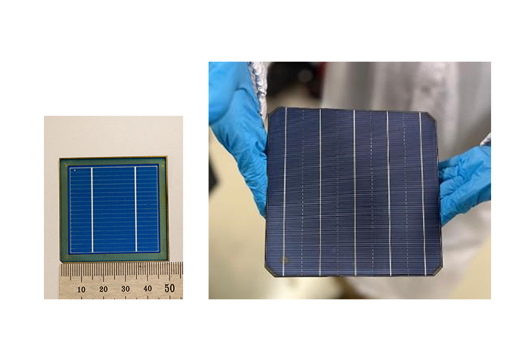
Fig. 2: Fig. 2: Photographs of SERIS-made perovskite-silicon 2T tandem solar cells. Left: 16-cm² (active area) device on a 25-cm² smooth silicon substrate. Right: M2-size (244 cm²) full-wafer tandem cell with textured silicon surface.
The current-voltage curves of a 16-cm² tandem cell measured at SERIS and a schematic of the cross-sectional device structure are shown in Fig. 3. The cell has an efficiency of 28.2%, which is a very good result considering that the top surface of the silicon bottom cell is smooth (i.e., not textured), which limits the current that can be generated by the silicon cell. The top cell’s perovskite absorber layer has a bandgap of 1.68 eV and was deposited using the spin-coating method. During spinning the wet precursor film spreads uniformly across the surface and undergoes rapid and controlled crystallisation, leading to large well-formed crystal grains with few defects. This results in a high electronic quality of the absorber layer and enabled the NISCM team to achieve more than 28% tandem cell efficiency on 16 cm², up from 25% a year earlier.
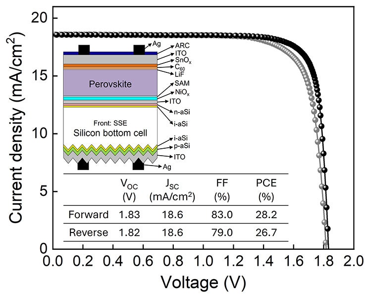
Fig. 3: Measured 1-Sun J-V curves of a 28.2% efficient perovskite-silicon 2T tandem solar cell with active area of 16 cm². The inset shows a schematic cross section of the device structure. The heterojunction Cz silicon bottom cell has a smooth front surface and a pyramid-textured rear surface. The perovskite absorber was made by spin coating.
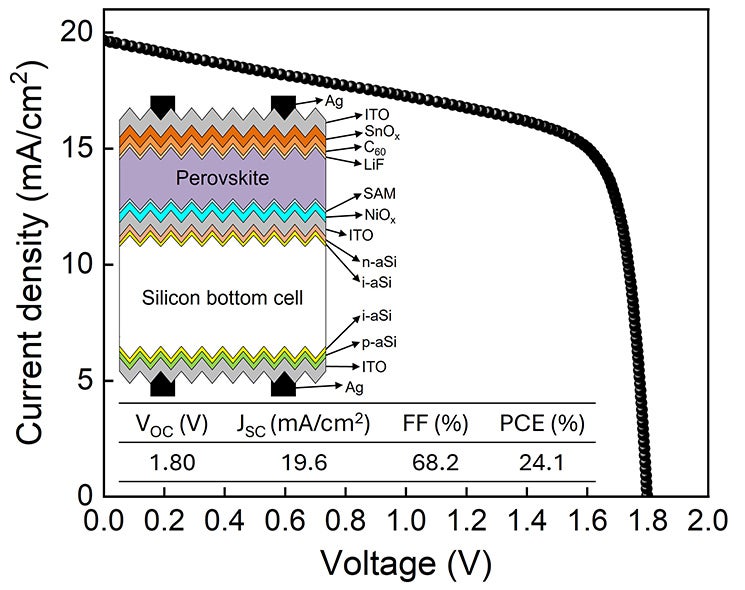
Fig. 4: Measured 1-Sun J-V curve of a 24.1% efficient perovskite-silicon 2T tandem solar cell with an area of 244 cm² (M2 size wafer). The heterojunction Cz silicon bottom cell has pyramid-textured front and rear surfaces. The perovskite absorber was made by a 2-step hybrid dry-wet processing sequence.
Using SERIS-made heterojunction silicon bottom cells on M2-size (244 cm²) Cz wafers with pyramid texture on both surfaces, the NISCM Cluster achieved 24.1% tandem cell efficiency in 2025, up from 20% a year earlier. The M2-size perovskite absorber layer of the top cell was produced via a 2-step hybrid dry-wet processing sequence, providing compatibility with upscaling to industrial wafer sizes and mass production workflows. The current-voltage curve of the 24.1% tandem cell and a schematic of its cross-sectional device structure are shown in Fig. 4. As can be seen, the open-circuit voltage (1.80 V) is good, but the fill factor is still rather low (~68%) due to a shunting issue. The NISCM Cluster’s ongoing efforts are focused on eliminating this top cell shunting issue and improving the tandem cell efficiency to more than 30%.
These achievements make SERIS the only facility in Singapore, and one of only a few labs in the world, capable of producing fully in-house fabricated high-efficiency perovskite-silicon 2T tandem solar cells on industrial-size silicon wafer substrates. In terms of power conversion efficiencies, SERIS maintained its position in 2025 as one of the top labs in the world for small (1 cm²), medium (~20 cm²) and large-area (> 200 cm²) 2-junction perovskite silicon tandem solar cells.
Development and upscaling of perovskite-silicon tandem cell mini-modules
In 2025, the project’s module team continued its work on the scaling of perovskite-silicon tandem cell mini-modules from lab-scale devices (1 cm²) to M2-size (244 cm²) prototypes. This process requires significant adaptation of our fabrication methods to meet the low thermal budget requirements imposed by the perovskite top cells. The Bill of Materials (BOM, see Fig.5) was optimised to ensure compatibility with low temperature processes below 120°C, without sacrificing efficiency.
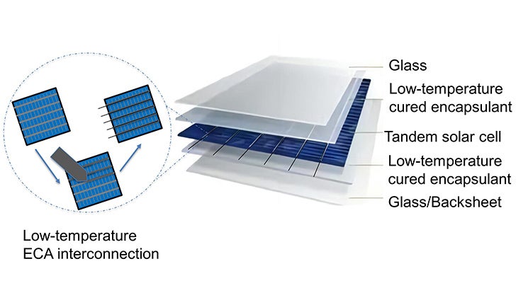
Fig. 5: Bill of Materials (BOM) for low-temperature fabrication of perovskite-silicon tandem cell modules.
The main achievement in 2025 was the fabrication and testing of M2-size perovskite silicon 1-cell tandem mini-modules with efficiencies of more than 21%, up from 16% a year earlier. Figure 6 shows a photograph of one of these fully in-house fabricated 244-cm² tandem mini-modules featuring low-temperature encapsulation and interconnections. This efficiency result was obtained through significant improvements in low-temperature encapsulation and interconnection technologies, specifically designed to meet the stringent temperature requirements of perovskite layers while reducing thermal stress and protecting structural integrity. The team screened and evaluated thermoplastic polyolefin (TPO) encapsulants for compatibility with perovskite layers, demonstrating high optical transmittance and minimal degradation after damp-heat testing, which is comparable to or better than that of conventional encapsulants. Stencil printed electrically conductive adhesives (ECAs) were optimised for low-temperature interconnections, enabling strong adhesion while minimising cell-to-module (CTM) losses.
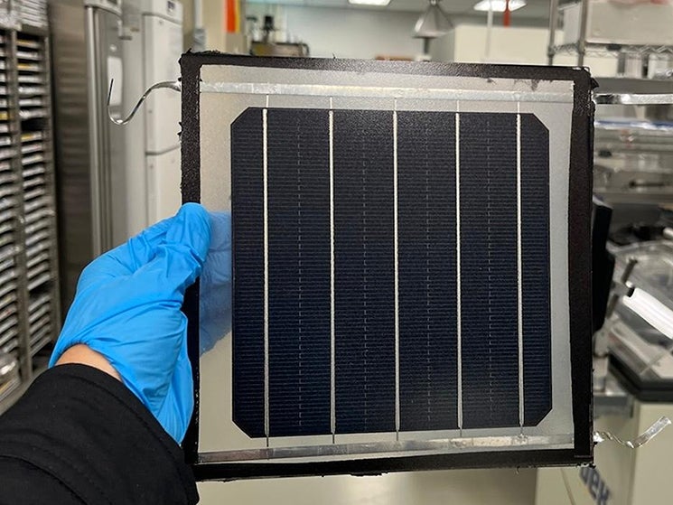
Fig. 6: Photograph of a fully in-house fabricated 244-cm² (M2- size) perovskite-silicon 1-cell tandem mini-module featuring low-temperature encapsulation and interconnections.
In 2025, the module team achieved the following technical milestones:
• Over 21% efficiency (with CTM losses of ~5%) for M2-size 244-cm² 1-cell tandem mini-modules. Using advanced materials (BOM) and encapsulation methods, we maintained the structural integrity and performance of these minimodules, marking an important step forward on the path to commercialisation of perovskite-silicon PV technology.
• Outdoor testing of tandem cell mini-modules (see Fig. 7): We started our outdoor tandem-cell mini-module testing activities at the NUS Rooftop Testbed in tropical Singapore in December 2024, using in-house fabricated tandem mini-modules. The initial tests highlighted the need for a stricter Bill of Materials in hot-humid conditions. In September 2025, the second batch of tandem mini-modules with optimised BOM for the tropics was deployed for continuous Jsc logging, temperature/irradiance monitoring, and monthly indoor stabilised I-V and spectral response measurements. Initial results show no significant degradation, with continuous monitoring ongoing to validate long-term stability.
• Indoor stability testing of tandem mini-modules: In June 2025, we initiated indoor testing of tandem modules under accelerated stress conditions. This includes damp-heat exposure, thermal cycling, and continuous maximum power point tracking (MPPT) under controlled irradiance and temperature conditions. We use in-house fabricated perovskite-silicon 1-cell tandem mini-modules for these tests. The primary aim is to identify possible degradation pathways and failure modes. We also aim to correlate these findings with outdoor data to provide accurate module lifetime predictions.
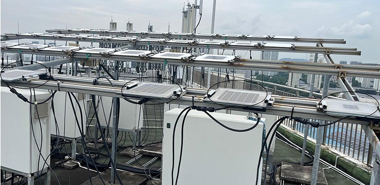
Fig. 7: Perovskite-silicon tandem mini-modules deployed at the NUS Rooftop Testbed for outdoor testing in Singapore’s hot-humid tropical climate.
Path Forward: Towards a 60-cell perovskite-silicon tandem module
The R&D roadmap of this flagship project involves the scaling up of 1-cell perovskite-silicon tandem mini-modules to 60-cell (~1.7m²) tandem modules by March 2027. Current efforts are focused on improving the durability of the low-temperature encapsulants and ECAs while adapting the processes to industry-compatible methods. We are conducting climate chamber testing and MPPT testing under controlled illumination and temperature conditions to refine our processes and improve the PV efficiency and durability of these novel tandem modules. This is complemented by ongoing outdoor testing of the prototype modules in Singapore’s hot and humid tropical climate, with emphasis on correlating indoor (damp heat, thermal cycling, and MPPT) and outdoor field data to predict degradation rates and guide BOM choices. Overall, this tandem flagship project is progressing well and is making major contributions to bringing the perovskitesilicon tandem PV technology closer to commercial viability, with the potential to deliver very-high-efficiency (30%) PV modules optimised for space-constrained environments like Singapore.
(2)Building-integrated Photovoltaics (BIPV)
Dr Carlos CLEMENT, Dr CHEN Tianyi, Srinath NALLURI, Rupendra ARYAL
Solar deployment in Singapore has grown strongly, from an installed DC capacity of 429 MWp (Megawatt-peak) of photovoltaic (PV) panels in 2020 to 1.64 GWp in Q2-2025. At the
current rate, the nation is projected to exceed its target of at least 2 GWp (Gigawatt-peak) installed DC capacity by 2030. However, this translates to only about 3% of Singapore’s annual electricity consumption, and there remains a need to further expand PV deployment. Singapore has an estimated PV installation capacity of 8.6 GWp (DC) within its territorial boundaries. Of this, approximately one third is attributed to rooftop PV (see Fig. 1), which is also the predominant form of PV deployment here.
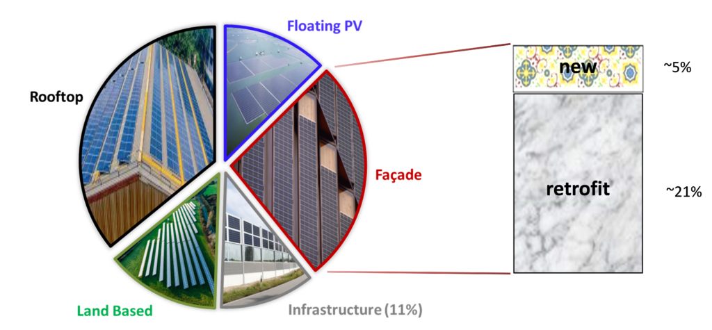
Fig. 1: Distribution of PV installation capacity in Singapore
Fig. 1: Distribution of the techno-economic solar potential for PV deployment based on the Solar PV Roadmap of Singapore 2020.
While there still remain significant unexploited rooftop spaces in Singapore, several challenges could hinder the full uptake of its potential, for example competing uses with building utilities (M&E equipment, chillers, antennas) or an increasing trend towards green roofs. Therefore it is ever more important and timely to address the second-largest solar potential shown in Fig. 1, which are façade areas by means of Building-integrated PV (BIPV) or Building-added PV (BAPV), collectively termed BIPV here. The techno-economic potential for facades entails an estimated 13.98 km2 of deployable area (~38% of total PV potential), however there are major barriers for the adoption of BIPV, including reluctance from architects due to concerns about aesthetics, higher costs, fire safety and integration complexity.
Pixel PV
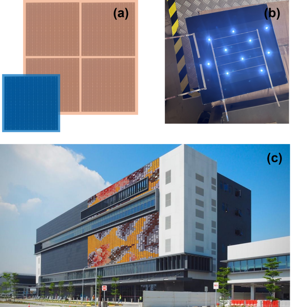
To further advance aesthetics and adaptability in BIPV, SERIS has developed and patented the Pixel PV concept, which reimagines conventional large-format panels (>2 m²) as smaller modular “pixels.” These pixels can be mass-produced in uniform colours or tile-inspired designs and then assembled into mosaic-style façades, providing both cost efficiency and creative freedom for architects (see Fig. 2). Beyond aesthetics, the smaller unit size also allows the system to adapt seamlessly to diverse façade dimensions and architectural form factors, reducing unutilised space and improving overall design flexibility. In 2025, the team continued product development of Pixel PV modules and has begun engaging industry partners to refine the technology toward commercialisation.
BIPV test-bedding
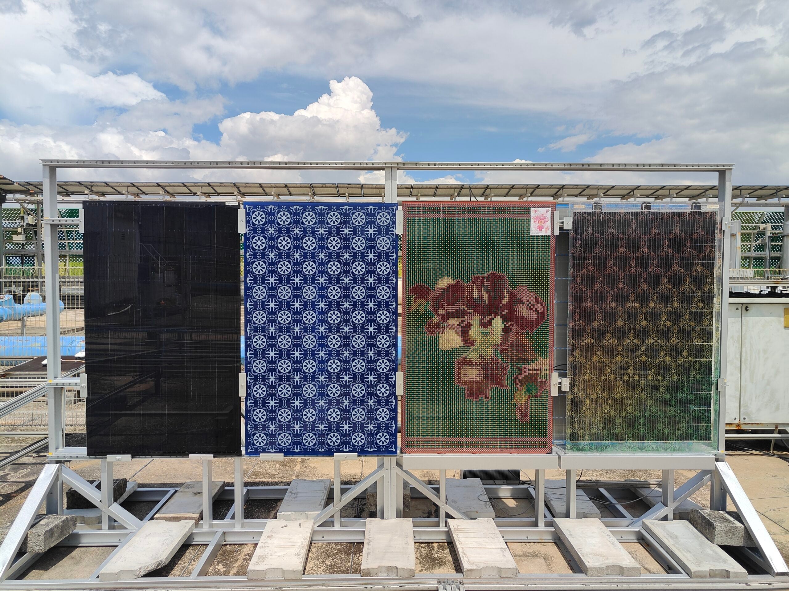
SERIS has built a dedicated outdoor BIPV testbed at the CleanTech One rooftop (see Fig. 3). The facility consists of two vertical walls, each measuring 5 m by 2 m, oriented to cover
all four principal directions. Designed with versatile attachment points and a modular, swappable façade system, the testbed enables flexible installation and evaluation of diverse BIPV technologies and mounting strategies. An advanced monitoring system has also been deployed, capturing high-resolution meteorological and irradiance data, alongside real-time electrical performance and sensing measurements. This platform is now fully operational and will support the systematic testing and validation of next-generation BIPV solutions under real-world conditions.
Building information modelling (BIM)
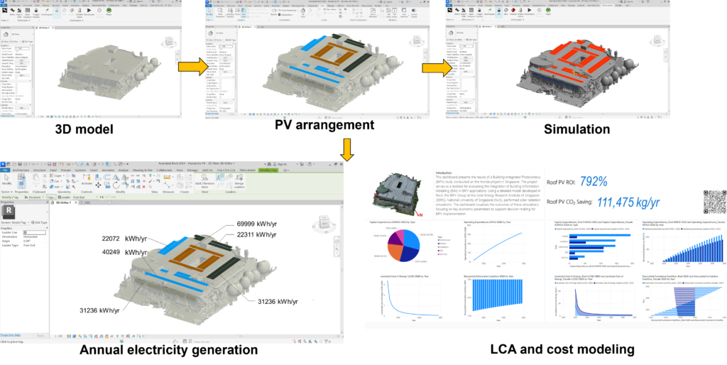
Another key challenge for BIPV adoption is the lack of a digital workflow within the standard BIM (Building Information Modelling) framework to streamline design and execution processes across project stages. The BIM system entails creating and managing digital representations of a building’s physical and functional characteristics (“digital twin”). This includes geometric models, time scheduling, cost and energy estimates and building operations.
In 2025, the team advanced this work by creating a digitalised BIPV component library within Revit, enabling direct integration of BIPV products into BIM workflows (see Fig. 4). The library allows architects and planners to populate 3D building models with PV elements, including façade-integrated systems, and run annual electricity generation simulations. These outputs are further linked to life cycle assessment (LCA) and cost models, providing early-stage insights into the performance, environmental impact, and economic feasibility of BIPV installations. By embedding BIPV elements at the conceptual design phase, this work lowers barriers to adoption, improves cost competitiveness compared to late-stage retrofits, thereby supporting Singapore’s Green Plan 2030 target of driving low-carbon, energy-efficient buildings.
BIPV as Art
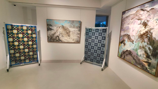
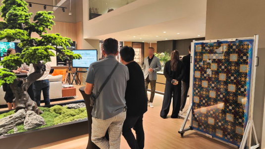
As part of our efforts to promote BIPV as both an attractive and practical solution for façades in Singapore, the team has been actively showcasing innovative displays at major events. In May, during the Art and Sustainability: A Shared Canvas exhibition, our Peranakan-inspired PV panels were presented alongside contemporary pieces of art at The Artworks Gallery (Fig. 5). In addition, our modules were featured at the Boloni Experience Center through a collaboration with Sunollo, interior design firm KAPA, and Porsche, highlighting the seamless integration of BIPV into modern design and lifestyle contexts (Fig. 6).
For further information, please contact:
Dr Carlos CLEMENT
carlos.clement@nus.edu.sg
Srinath NALLURI
srinath.nalluri@nus.edu.sg
Rupendra ARYAL
rupendra@nus.edu.sg
(3)Floating Solar Systems
Dr Serena LIN Fen, Dr Oktoviano GANDHI, Lokesh VINAYAGAM, Dr Thomas REINDL
Floating photovoltaics (FPV) offers great opportunities for renewable energy generation, particularly for countries with land constraints and available water bodies, such as Singapore, South Korea, Japan and the Netherlands. SERIS has been leading the Floating Solar research in Singapore and worldwide since 2016, and has created and maintained a FPV system database of around 1600 installations to date.
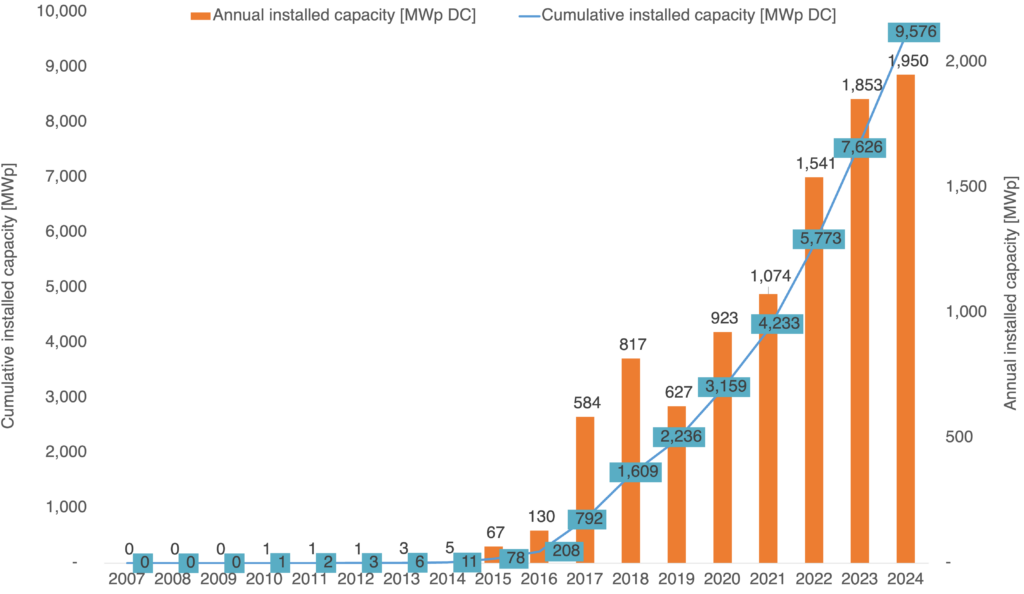
At the end of 2024, the cumulative installed global FPV capacity had reached around 9.5 GWp (see Fig. 1). Despite the rapid deployment of FPV systems in the last 10 years, the current global installed capacity is still far below its potential. By covering just 10% of the > 250000 inland water bodies worldwide, FPV could reach an installed capacity of ~23 TWp and a potential energy yield of around 25000 TWh/year, which is equivalent to the total global electricity demand in a year (2023 data). This demonstrates the huge potential of reservoir-based FPV in the future.
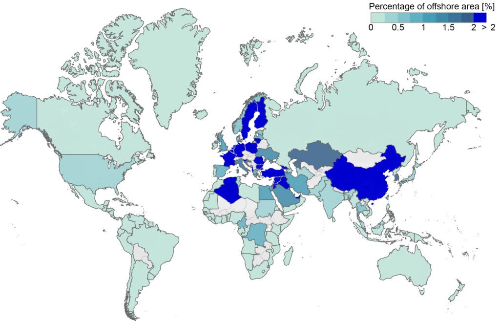
a) Offshore area required
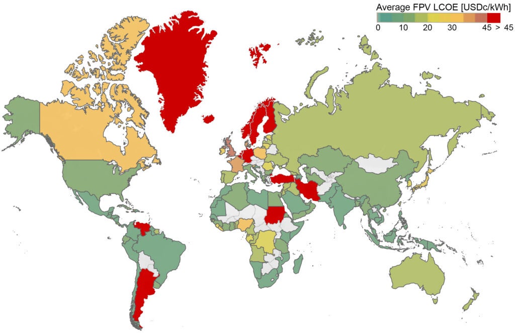
b) Average OFPV LCOE
In comparison with reservoir-based FPV, the potential for offshore FPV (OFPV) is even larger. A SERIS assessment showed that - even when limiting the ocean regions to conditions that can be withstood by current commercial floater capabilities, excluding protected areas and dense shipping routes - a 10% coverage would already provide about 686 TWp
of FPV capacity. Due to this enormous potential, less than 2% of the available offshore water surfaces are sufficient to meet the current electricity demands of 84% of the analysed regions. Moreover, in 53% of the analysed regions (see Fig. 2), the required FPV water area to satisfy their electricity demand corresponds to an OFPV LCOE of below 15 USDc/kWh, underscoring OFPV’s potential cost competitiveness.
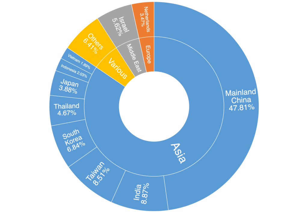
Even though the presently installed FPV capacity is concentrated in only a handful of regions (see Fig. 3), FPV is a global phenomenon, with 66 countries hosting FPV installations at the end of 2024, and many more with projects under development.
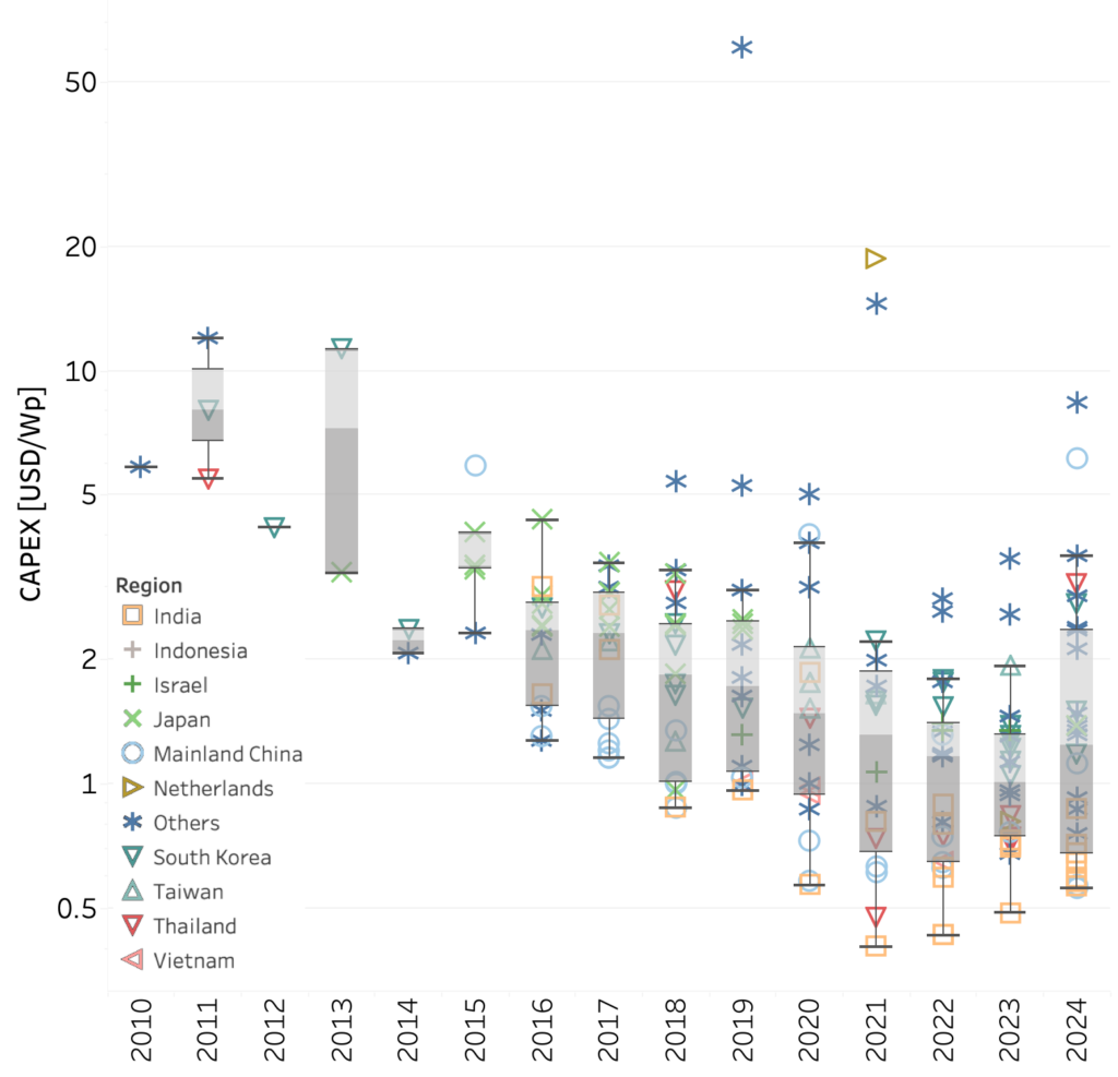
The increase in FPV installations, along with the advancements in technology, has brought down FPV cost from a median of 2.41 USD/Wp in 2015 to 1.25 USD/Wp
in 2024 (see Fig. 4), which enabled even wider FPV adoption. The median CAPEX in 2024 experienced an increase from 2023 despite a drop in module prices, partly due to inflation.
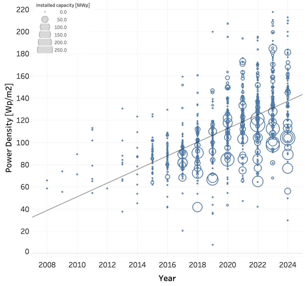
At the same time, the increase in module efficiency has allowed higher power density for FPV installations (from a median of 88Wp/m2 in 2015 to 139 Wp/m2 in 2024, as illustrated in Fig. 5). Incremental increases in module efficiency and FPV deployment experience will increase FPV potential further in the coming years.
Such insights from our FPV database are regularly presented by SERIS in conferences and exhibitions and are highly valued by the industry. To share its knowledge, SERIS has published the “Where Sun meets Water” report series, together with the World Bank Group. By October 2025, downloads of these reports from the World Bank sharing website (ESMAP) had surpassed 160,000, underlining the high relevance of these reports for the solar industry.
SERIS’ Floating Solar flagship project has adopted a holistic approach towards driving various aspects of the FPV industry, which is summarised in Fig. 6 and explained in more detail in the following sections.
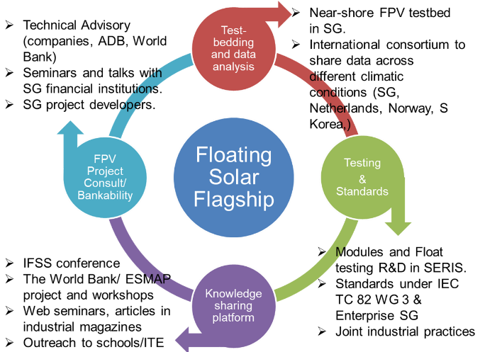
FPV test-bedding and data analysis
Floating PV systems deployed in sea water (either near-shore or off-shore) are the next frontier in scientific PV systems research at SERIS, following a growing interest in Singapore and around the world to utilise marine areas for Floating Solar. This could lead to a virtually unlimited availability of space, provided that there are cost-effective and reliable technologies for deployment as well as for the interconnection to shore. However, this market segment is at a very nascent stage and there is limited information about technical designs, component selection, feasibility, and field data available today to estimate the economic viability of marine-based floating PV systems. Sea conditions pose additional challenges - such as higher wind and wave forces (and their combined effects), salinity of seawater, and biofouling - that will affect the mechanical stability of the floating structures. Moreover, depending on the distance from the shore and the water depth, the anchoring and mooring engineering becomes more complex and thus expensive. There are solutions available in the marine industry to overcome certain technical challenges, but they need to match the cost levels required by the PV industry to ensure that FPV power is competitive with other forms of renewable energy generation.
FPV testing & standards
SERIS previously led the development of Singapore’s national FPV standard, TR100:2022 – Floating photovoltaic power plants: Design guidelines and recommendations, in collaboration with Enterprise Singapore (E-SG). With this national guideline now established and widely adopted by the local industry, SERIS has shifted its focus towards international standardisation to support the global FPV market.
In 2025, SERIS continued to play a key role in the development of the first international FPV standard through IEC TC82 Working Group 3. SERIS presented the initial draft of IEC 62548-3: Floating Photovoltaic (FPV) Arrays – Design Requirements at the Spring 2025 WG3 meeting in Singapore, and is working closely with international partners toward its finalisation. The IEC work is being coordinated with ongoing standardisation efforts across the industry, including contributions from marine engineering, materials, and component-level technical domains, as well as parallel activities within IEC TC82 WG2 on FPVspecific PV module requirements. Together, these initiatives aim to establish a harmonised and comprehensive framework for FPV system design, strengthening the overall quality, durability, and bankability of FPV installations worldwide.
Knowledge sharing platform
As one of the leading research institutes in floating solar, SERIS’ knowledge and expertise are highly sought after in the international PV community. In 2025, SERIS has been invited to major international PV conferences held in various countries, such as China, Germany, Spain, Thailand, South Korea and Singapore, to share the latest trends in Floating Solar, as well as the results of its research on topics such as FPV potential, reliability, and operation.
SERIS has shared its experiences not only with academia and industry, but also with the wider solar community, by giving lectures on Floating PV, such as in the “Sun Powered Future” webinar organised by Asian Development Bank and the two “Renewable Energy Futures” webinars organised by the Society of Floating Solutions (Singapore) on “Floating Solar PV Potentials in Malaysia and Operators’ Experience” and “Floating Solar PV Systems in Indonesia”.
FPV technical advisory
Although many FPV projects are now in operation or under construction globally, there is still a lack of technical knowledge in the industry. SERIS has been working with major developers and multi-national lenders such as the World Bank Group (World Bank, IFC), the Asian Development Bank (ADB), the InterAmerican Development Bank (IADB) and the United States Agency for International Development (USAID) on projects in Singapore, Pakistan, India, Sri Lanka, Vietnam, the Philippines, Suriname, Tuvalu, Micronesia and Mexico to transfer its knowledge to their real-world projects, be it as part of feasibility studies, the engineering design work, or preparation of technical documents for tender specifications. As of 2025, SERIS was involved in the feasibility studies and the design of ~3.0 GWp of FPV system.
Dr Serena LIN Fen
lin.fen@nus.edu.sg
Dr Oktoviano GANDHI
okto@nus.edu.sg
Lokesh VINAYAGAM
servl@nus.edu.sg