
This laboratory is located on levels 1 and 2 of the E3A building on the main NUS campus. Equipped with Industrial-scale tools capable of processing more than 100 wafers per hour, it enables industry-relevant R&D on solar cells using monocrystalline silicon wafers.
Silicon Cleanroom Lab 1A
Lab 1A is dedicated to wet-chemical processing of silicon wafers. It is equipped with highly versatile R&D equipment for developing advanced processes aimed at high-efficiency Si solar cells as well as Si bottom cells for application in perovskite-silicon tandem cells. The lab also houses industrial-scale high-throughput wetchemical process tools, enabling rapid technology transfer to industry.
Manual Batch Wet-Benches (MediaMac, Singapore)
These batch wet-chemistry tools, custom-built by MediaMac, are designed for flexibility and precision in silicon solar cell process development. They feature versatile process baths for developing various wet-chemical processes (cleaning, texturing, etching) related to silicon solar cell processing. The tools can process up to 50 silicon wafers per batch, with wafer sizes up to M10 and half-cut G12, enabling seamless scalability from lab to industry.
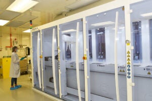
Automated Batch Wet-Chemistry (BatchTex, RENA Technologies, Germany)
The BatchTex tool from RENA Technologies is a high-throughput (> 250 wafers/hr), automated wet-chemical processing system for etching, alkaline texturing and cleaning of silicon wafers (up to M10 size and half-cut G12). It features multiple process baths with automated bleed and feed function, ensuring stable chemical concentrations and exceptional process consistency via real-time sensors. The tool also has state-of-the-art O3 - based wet-chemical baths. It enables advanced wafer cleaning, producing tailored surface morphologies and the formation of thin oxide films. The integrated robotic arms ensure fast, safe and uniform wafer processing, delivering reliable performance and industry-ready results.
Inline Wet-Chemistry (InPilot, RENA Technologies, Germany)
The InPilot tool from RENA Technologies is an inline wetchemistry processing system designed for single-side etching of silicon wafers (up to M10 size and half-cut G12). This is a semiautomated single-lane machine for inline wet-chemical etching. It comprises an HF bath, an alkaline bath, and an acidic bath for single-sided wafer etching, with a water rinse section to ensure process purity and consistency. Both the HF and alkaline baths can be heated separately, allowing precise control over etching conditions and surface quality.
Silicon Cleanroom Lab 1B
Lab 1B houses several chemical vapour deposition (CVD) tools capable of depositing a wide range of thin-film materials, with thicknesses ranging from a few atoms thick to several hundred nanometres.
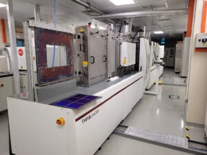
Inline dynamic PECVD tool (MAiA 2.1 / Meyer Burger, Germany)
The MAiA 2.1 from Meyer Burger is an R&D inline plasmaenhanced CVD (PECVD) machine designed for quasicontinuous, high-throughput operation – achieving processing speeds of over 1000 wafers per hour for selected processes. The
thin-film deposition process uses a ‘remote’ plasma energised by 2.54-GHz microwaves, which minimises plasma-induced wafer damage compared to the conventional parallel plate designs. The loading module is equipped with an infrared lamp array for rapid substrate heating to the desired process temperature (350-550ºC). The machine is capable of depositing silicon nitride (SiNx), silicon oxide (SiOx) and aluminium oxide (Al2O3) thin films onto large silicon wafers (M2 to G12).
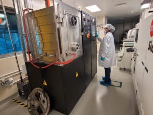
Spatial ALD tool (Manual ALD Lab tool / SoLayTec, Netherlands)
This manual ALD Lab tool from SoLayTec is a pioneering R&D system for the deposition of Al2O3, intrinsic ZnO, Al-doped ZnO and SnO thin films using the spatial atomic layer deposition (sALD) technology, where precursors are separated in space rather than in time. This versatile tool is able to deposit thin films onto a wide range of substrate types and sizes (up to G12 size wafers or 21 cm x 21 cm glass panes). Al2O3 films play an important role in advancing various silicon solar cell technologies, while ZnO and SnO based films enable the development of transparent conductive oxides or transparent metal oxides for high-efficiency large-area perovskite-silicon tandem solar cells.
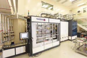
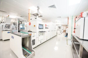
Versatile Tube furnace (TS81254 / Tempress Systems, Netherlands)
The TS81254 from Tempress Systems is a 4-stack highthroughput R&D tube furnace with several capabilities:
• Low-pressure chemical vapour deposition (LPCVD) of doped
& intrinsic poly-Si films for passivated-contact solar cell
applications (double-sided deposition)
• Deposition of doped & intrinsic silicon nitride films
• Oxidation process for advanced surface passivation applications
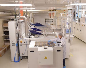
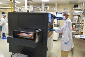
PECVD tool for ultra-fast deposition of doped silicon and metal oxide thin films (CAiA Lab, Meyer Burger, Germany)
The CAiA Lab tool is a unique prototype PECVD machine for the ultra-fast deposition of intrinsic and doped silicon thin films and associated stacks, as well as doped transparent metal oxide films. It was jointly developed by SERIS and Meyer Burger. The tool has two process chambers to prevent cross-contamination. It enables the single-sided deposition of thin high-quality interfacial oxide layers and low-absorbing and dense doped-layer stacks on large silicon wafers (M2 to half-cut G12). The tool is used for cutting-edge R&D on single-junction silicon solar cells as well as tandem devices incorporating a silicon bottom cell.
![]()
PECVD tool for the deposition of intrinsic and doped (boron, phosphorus) amorphous silicon layers (Octopus II, INDEOTEC SA, Switzerland)
The Octopus II is a state-of-the-art PECVD tool for the deposition of intrinsic and doped (boron, phosphorus) a-Si layers for applications in heterojunction silicon solar cells. The machine is capable of processing up to G12-size silicon wafers and is designed in a cluster form to provide the process flexibility needed by the R&D activities. The tool is also able to deposit various nanocrystalline layers like nc-Si, nc-SiOx and nc-SiC.
Silicon Cleanroom Lab 2A
Lab 2A houses tools for precision and advanced processing of high-efficiency solar cells. It features a versatile laser tool and an inkjet printing tool, enabling the creation of sophisticated cell features with high accuracy and flexibility.
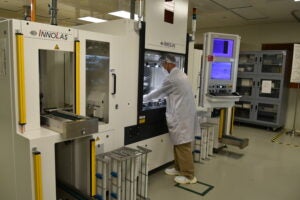
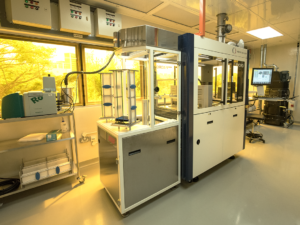
Versatile Laser System (ILS LT 124 / Innolas Solutions, Germany)
The ILS LT is an R&D laser processing workstation for highprecision applications in PV. The machine features three laser sources to provide excellent flexibility: a 2-W UV continuous source, a 20-W green ns source, and a 30-W fs source that can be tuned to operate at either UV, green or IR wavelengths. This configuration enables several process applications for high-efficiency solar cells, including contact opening, selective mask processing or edge/junction isolation, wafer drilling, wafer cutting, silicon shadow mask fabrication and laser marking for substrate ID tracking purposes. The tool has automated handling for substrates up to M6 size, and is also capable of processing larger wafers (up to G12 size) using manual handling.
![]()
Pilot-scale Inkjet Printer (IP410 / Meyer Burger, Netherlands)
The IP410 is a versatile pilot-scale inkjet printer designed for solar cell masking and patterning applications. It supports a wide range of functional inks, including hotmelt inks, UV curable inks, solvent-based metal inks, and chemical precursor inks (e.g. for perovskite cells). Multiple printing modules are available to quickly switch between different ink types while preventing cross contamination. An ink evaluation module with disposable cartridges allows the testing of small volumes of experimental inks. Printing patterns are digitally defined and thus can be quickly updated, which makes the machine ideal for process development and rapid prototyping. It is fully automated and includes cassette loading and unloading of wafers up to M6 size. Manual handling of larger wafers (up to G12) is also possible.
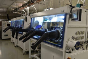
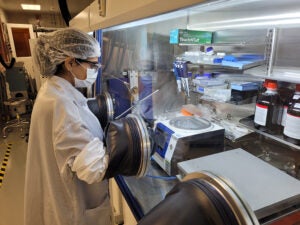
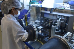
Lab 2A Glovebox Setup (Mikrouna, China)
A 3-section glovebox setup provides the controlled, moisture-free environment required for the processing of moisture-sensitive materials. This setup accommodates an inkjet printer, a spin coater, a hotplate and a chemical storage area. The integrated design ensures seamless contamination-free transfer of the samples throughout the system.
Pilot-Scale Inkjet Printer (PiXDRO / SUSS MicroTec, Netherlands) in a glovebox
The PiXDRO inkjet printer in the glovebox setup is a pilot-line tool capable of handling substrates up to G12 size, making it ideal for the precise deposition of moisture-sensitive films such as perovskite and charge transport layers for industrial-size perovskite-silicon tandem solar cells. Supporting a wide range of functional inks, the PiXDRO printer enables rapid switching between ink types with minimal risk of cross-contamination, offering excellent flexibility for advanced process development.
Spin Coater (LEBO Science, China) in a glovebox
This spin coater, paired with a hotplate, is housed in a separate section of the glovebox setup. This configuration ensures uniform deposition and curing of perovskite and other functional layers, enabling precise and high-quality layer formation for advanced solar cell development.
Silicon Metallisation Lab 2B
Lab 2B facilitates metallisation and contact formation for various types of solar cells. Equipped with several advanced metallisation tools, it caters to both high- and low-temperature processes, enabling precise and efficient fabrication of high-performance solar cells.
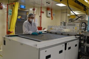
R&D screen printer (ASYS, Germany)
This versatile R&D screen printer from ASYS is capable of screen printing metal contacts onto a wide range of substrate sizes, ranging from small (5 cm x 5 cm) to very large (21 cm x21 cm, G12). The printer is also capable of stencil printing for added flexibility. It is equipped with a patented vision alignment lens capability, i.e. a smart assistance system, which uses a free-moving camera and thus provides a lot of flexibility for aligning the substrates. This enables a repeatability of ± 10 µm by utilising a high-precision measuring system and an automatic screen adjustment system.
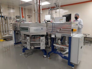
Fast firing furnace (SinTerra / BTU, USA)
The SinTerra is an automated fast firing furnace from BTU/ AMTECH Systems. It is equipped with automated cassette loading & unloading and has 6 zones with infrared lamps for
heating silicon wafers (up to M6 size) to temperatures in the 300- 1000°C range. Ramp-up and ramp-down rates can be precisely controlled in order to tailor the firing profiles.
Thermal Evaporator (SCT / System Control Technologies, USA)
The SCT thermal evaporator is a lab-scale tool for evaporating thin films of metals (Al, Ag, etc) and other materials onto various substrates (wafers, glass panes, etc) of sizes up to G12. The deposition chamber uses a cryogenic pump to achieve a very low base pressure (< 10-6 Torr), ensuring high-purity films. The evaporator features dual resistively heated sources and a rotating substrate holder to ensure uniform depositions across large-area substrates.
Inline multi-chamber sputter machines #1 and #2 (SV-540 & Line-540, FHR Anlagenbau, Germany)
This physical vapour deposition (PVD) sputtering platform is
designed to handle silicon wafers and glass panes. Substrates
of sizes up to 30 cm x 40 cm or up to six M6-size or four half-cut
G12 wafers can be processed per run.
The SV-540 tool has dedicated processing chambers for the sputtering of metallic, dielectric and TCO/TMO layers. They are equipped with planar magnetron sources for DC and RF
sputtering of metals, oxides and oxynitrides in the reactive mode, and with a cylindrical dual-magnetron source and planar sources for pulsed DC (“DC+”) sputtering of dielectrics and TCOs/TMOs, with substrate heating up to 400ºC. It is also possible to deposit graded layers, or multi-layer stacks of up to 6 different materials, without breaking the vacuum conditions. Materials that can be sputtered include indium tin oxide, aluminium-doped zinc oxide, Ag, Al, Ti, In, ZnO and thin oxide and oxynitride films tuned to specific requirements. The Line540 tool has 3 planar magnetron sources, whereby 2 are connected to a DC power supply for DC sputtering of metal layers, while the third is connected to an RF power supply for the deposition of metal oxide films such as NiOx, Mg:NiOx, iZnO andMgZnO4. The substrates can be heated up to 200ºC in this tool.
- Overview of Facilities & Labs
- Perovskite Solar Cell Laboratory
- Silicon Solar Cell Laboratory
- Photovoltaic Devices Characterisation Laboratories
- PV Devices Modelling and Simulation
- PV Module Development Laboratory
- SERIS’ ISO/IEC 17025 Laboratory For Module Testing
- Outdoor PV Module And System Testing Facilities In Different Climates
- PV Systems Monitoring Laboratory
- Electronics Laboratory