Magnetron Sputtering of Metal and Transparent Conductive Oxide (TCO) Coatings for Industrial Prototyping
Magnetron sputtering is a vacuum-based physical vapour deposition (PVD) process that is widely used in the coating industry to deposit thin films onto various substrates (glass, foil, steel, etc), for a wide range of applications. SERIS is offering magnetron sputtering services for small numbers of samples to allow clients from industry and academia to explore the use of this versatile technology for their prototypes and products.
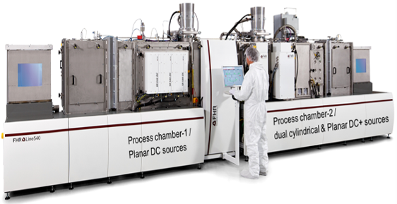
SERIS’ PVD sputtering platform is designed for medium- to high-throughput applications such as solar cells, architectural glass, and flat-panel displays. The machine can handle any flat substrate with a size of up to 300 mm x 400 mm, with a maximum thickness of 5 mm. Typical substrates would be glass and silicon wafers. This state-of-the-art machine has dedicated vacuum chambers for the sputtering of metallic, dielectric and transparent conductive oxide (TCO) layers. The processing chambers are equipped with planar magnetron sources for DC sputtering of metals, oxides and oxynitrides in the reactive mode, and with a cylindrical dual-magnetron source and planar sources for pulsed DC (DC+) and RF sputtering of dielectrics and TCOs, with substrate heating up to 400°C. This
allows to deposit thin layers of metals, TCOs and dielectrics onto various substrates. It is also possible to deposit graded layers with varying refractive index, or multi-layer stacks of up to six different materials, without breaking the vacuum conditions. As the platform is comparable with large-scale production machines, processes developed on this machine can easily be scaled up to industrial production lines. At SERIS we use this tool for depositing metal layers, TCOs and multi-layers for silicon and thin-film solar cells, as well as perovskite-Si tandem solar cells. The main features of our sputtering machine are listed in Table 1.
In addition to AZO and ITO, we are able to deposit a variety of other layers, including Ag, Al, Ti, In, ZnO, IZO, NiOx, Mg:NiOx and thin layers of metal, oxide and oxynitride tuned to customer requirements.

Table 1. Process capabilities of the in-line sputtering machine at SERIS
| Parameter | Details |
| Substrate | Glass, Si wafers and foils |
| Substrate size | Minimum 50 mm x 50 mm, maximum 300 mm x 400 mm |
| Substrate movement | Linear and oscillating |
| Substrate temperature | Up to 400°C |
| Power supply | DC , DC+ (0 - 10 kW) and RF (0 to 2 kW) |
| Sputter targets | Planar (Ti, Zn, Ag, Al, ITO)
Dual cylinder (2 wt % Al doped ZnO) |
| Gas supply | Ar, O2, N2, Ar+O2 (98% + 2%) |
| Layers | Ag, Al, TiO2, ZnO, AZO, ITO |
For further information, please contact:
Dr Selvaraj VENKATARAJ
Corporate Laboratory Group
NISCM Cluster

