An efficient solar cell maximises the conversion of photons in the sun’s spectrum into energetic charge carriers, and minimises undesirable recombination processes that reduce the cell’s current and voltage output. SERIS is equipped with a comprehensive suite of tools that can deduce the optical properties (related to photon-to-charge carrier conversion) and electrical properties (related to charge carrier recombination) of solar cells and materials. Technology Computer-Aided Design (TCAD) process and device simulators, as well as large-area network model representations of the solar cells are used extensively to trace the origins of the measurement features to the layers and structures of the cell, analyse them, and predict the potential for efficiency improvements with respect to process or cell design changes.
Sample testing and analysis
(see also PHOTOVOLTAIC DEVICES CHARACTERISATION LABORATORIES)
• High-precision steady-state light I-V and spectral response measurements for solar cell devices
• Solar Cell Doctor: Detailed health check for solar cells
• Photoluminescence and electroluminescence imaging
• Determination of thickness and optical properties of thin films by spectroscopic ellipsometry
• Total and angular spectral transmittance and reflectance measurements by UV-VIS-NIR spectrophotometer.
• Steady-state and transient carrier lifetime characterisation by photoconductance and photoluminescence-based measurements
• Measurement of photoluminescence/fluorescence spectra and decay lifetime using time-resolved photoluminescence spectroscopy
• Absolute luminescence quantum yield measurement of thin-film stacks and devices
• Dopant profile determination by electrochemical capacitance-voltage (ECV) measurements
• Scanning electron microscopy, including cross-sectional elemental analysis by energy dispersive X-ray (EDX), and determination of crystalline grain orientation by electron back scatter diffraction (EBSD)
• Carrier concentration and carrier mobility determination of transparent conductive oxides, conductive films and semiconductor layers by the Hall effect
• Mapping of impurity zones and defects in silicon wafers
Solar Cell Doctor: Detailed health check for silicon solar cells
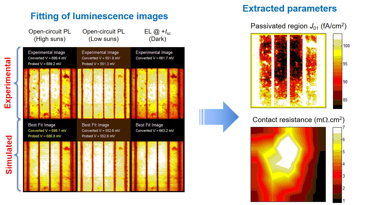
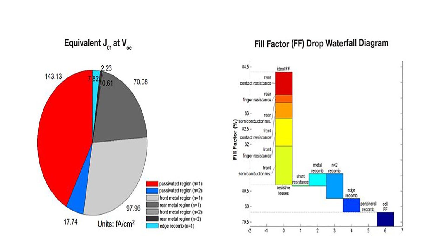
By combining solar cell characterisation methods with easy-to-make test structures and partially processed silicon solar cells from the production line, the Solar Cell Doctor loss analysis routine uses sophisticated computational methods to break down various cell loss mechanisms to generate process-related diagnostics. Exemplary analyses of several silicon solar cells are shown below. Fitting of specific luminescence images permits the extraction of the spatial distribution of the saturation current density J01 of the passivated cell region and the contact resistance. By creating an accurate representation of the solar cell under test, factors limiting the shortcircuit current density, open-circuit voltage and fill factor are identified. Design and process changes can also be evaluated in terms of their influence on the cell efficiency.


Analysis of next-generation solar cells
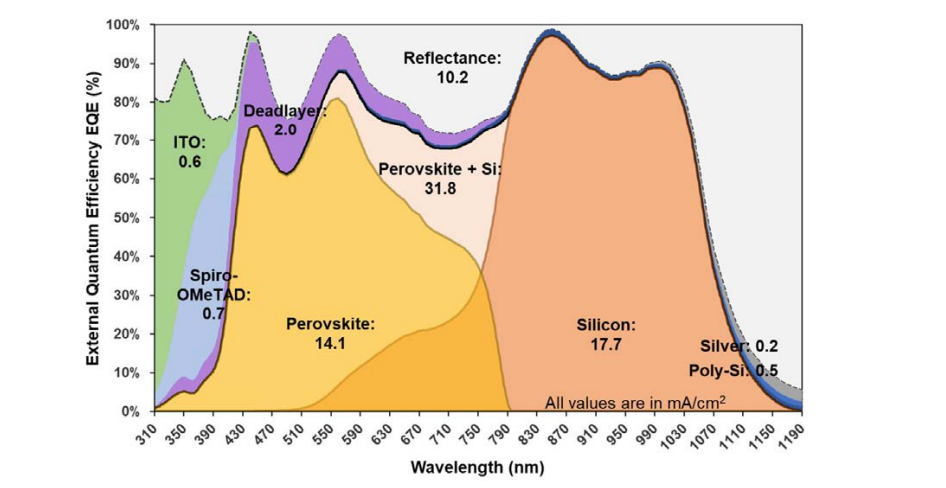
Through in-depth advanced solar cell/material characterisation and device modelling, SERIS has developed powerful loss analysis techniques that can be applied to next-generation high-efficiency solar cells such as perovskite thin-film cells and perovskite-Si tandem solar cells. The influence of various layers in the solar cell stack on electrical current losses can be clearly delineated. Studies of the impact of bulk and interface recombination can also be performed for the quantification of related voltage losses. Such analysis provides crucial information for material screening, understanding and optimising device performance.


