SERIS operates state-of-the-art industrial silicon solar cell processing equipment from leading manufacturers for its internal R&D. To support the global PV research community, we offer a range of processing services in our Silicon Solar Cell Lab to external customers. Selected examples of processing services for research-type silicon solar wafers and cells are listed below.
Processing of large-area silicon solar wafers and cells
- M2 to G12 wafer size (up to 210 mm ´ 210 mm)
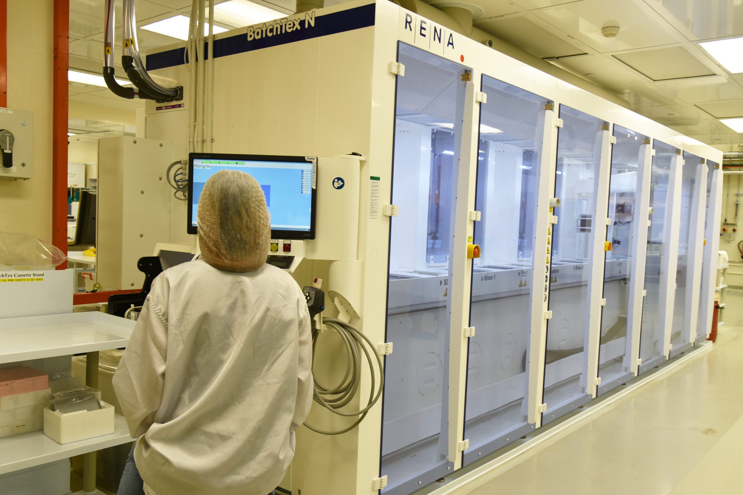
- Batch-type wet-chemical processes including cleaning, etching and texturing
- Inline wet-chemical processes (both acid and alkaline chemistries) including cleaning and etching
- PECVD of dielectric layers (SiNx, AlOx, SiOx, SiOxNy etc)
- PECVD of intrinsic or doped (boron, phosphorus) a-Si layers for applications in polysilicon based passivated-contact solar cells
- PECVD of intrinsic or doped (boron, phosphorus) a-Si layers for applications in silicon heterojunction solar cells
- ALD of Al2O3, SnO2 and AZO layers
- PVD of various thin films (metals, TCOs, TMOs) by sputtering and thermal evaporation
- Thermal processes including oxidation, forming gas anneal, co-annealing
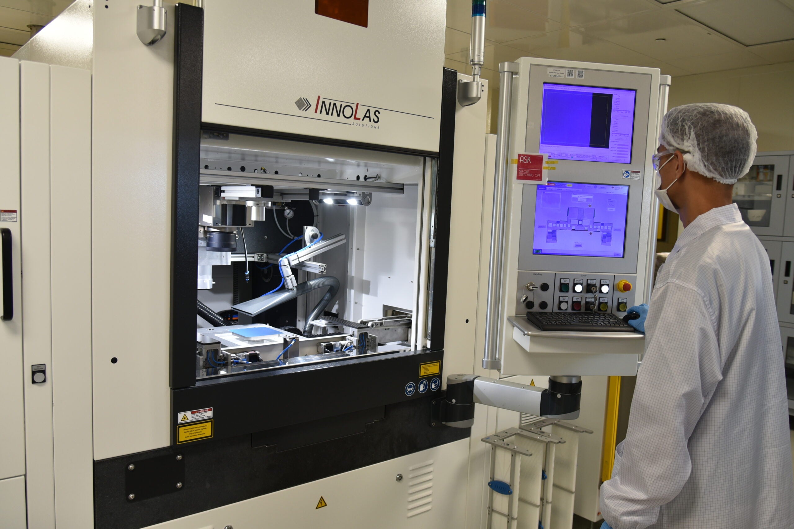
- Laser processing using ns pulses (green) and ps or fs pulses (UV, green, IR light)
- Inkjet printing of masking layers for patterning applications
- Screen printing of metal contacts (Ag, Al, Cu) and fast firing in a belt furnace

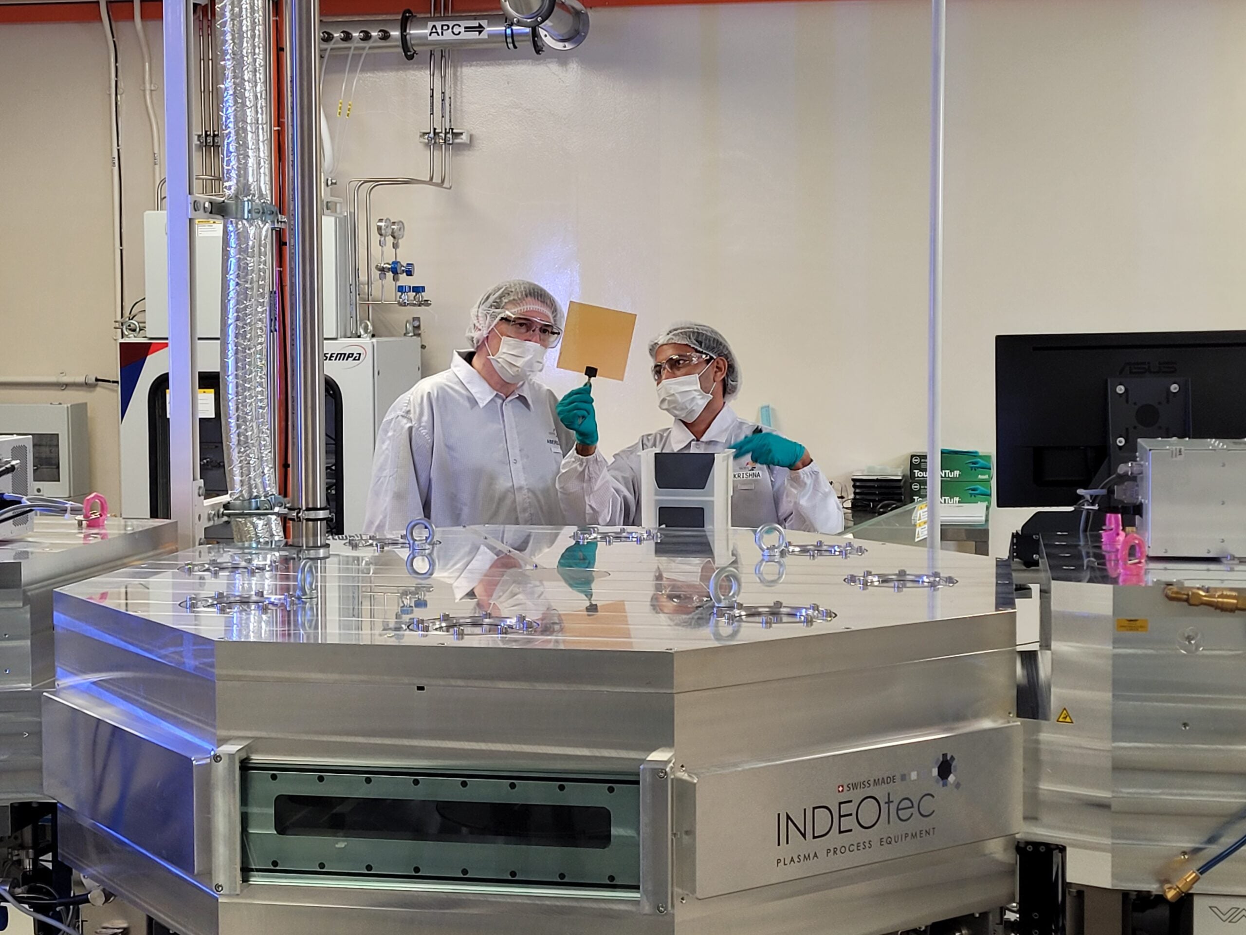
PECVD tool for deposition of intrinsic and doped amorphous silicon layers for applications in heterojunction solar cells.

Inline wet-chemical processes (both acid and alkaline chemistries) including cleaning and etching

Laser processing of silicon wafer solar cells using ns pulses (green) and ps or fs pulses (UV, green, IR light)

