Photovoltaic Devices Characterisation Laboratories

The PV Devices Characterisation Laboratories at SERIS are equipped with a comprehensive suite of measurement tools designed to examine both material and device properties. The characterisation of optical & passivation layers, bulk materials, and solar cell metallisation enhances the understanding of their impact on solar cell efficiency. This complements device-level measurements of perovskite-based and silicon-based solar cells, tandem cells, and single-cell mini-modules. By combining meticulous characterisation with specialised simulation techniques, advanced solar cell analysis can quantify performance-limiting factors and predict potential efficiency improvements.

Materials Characterisation Laboratory

This laboratory houses both general-purpose materials characterisation tools, such as 3D optical microscopy, FTIR and Raman spectroscopy, as well as silicon-based materials characterisation techniques, including a wafer thickness & resistivity measurement tool, an effective minority carrier lifetime tester, and a TLM resistance measurement tool. It also contains a small-beam spectral response measurement system to study the optoelectronic properties of solar cells, and a contactless corona-voltage measurement system for interface defect characterisation.

Materials Characterisation Laboratory

External quantum efficiency (EQE) and total reflectance (R) measurements enable detailed current loss analysis and the identification of areas for improvement related to diffusion lengths and light management. The PVE-300 allows quick and localised measurements of both EQE and R over a wavelength range of 300-1700 nm for various types of solar cells.

Measured EQE of a monolithic perovskite-Si tandem cell made by SERIS

Photoluminescence (PL) and electroluminescence (EL) tools are considered the "X-ray scanners" of the silicon PV community, capable of quickly producing luminescence images for routine inspections or detailed two-dimensional data sets used for sophisticated computational analysis.

The transmission line method (TLM) enables metal-semiconductor contact resistance measurements down to 1 mΩ-cm2. Different probe heads are available for a wide range of metallisation finger pitches, suitable for measuring both screen-printed solar cells as well as test structures with evaporated metal contacts. Busbar-to-busbar resistance and line resistance measurements are complementary techniques used to determine the metal grid resistance.

This technique provides fast contactless measurement of interface parameters that affect the passivation quality of dielectric films for PV applications. The metrological capabilities include the mapping of contact potential (in the dark or under illumination), band bending at the semiconductor/dielectric interface, fixed charge in the dielectric, and interface defect density. Microwave-detected photoconductance decay (μ-PCD) is a time-resolved method to determine and map the effective carrier lifetime of silicon wafer samples with a spatial resolution of 5 mm.

Electron Microscopy Laboratory

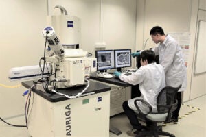
The centrepiece equipment of this laboratory is the FE-SEM (field-emission scanning electron microscope), an electron microscope used to obtain high-magnification images of submicron structures of electrically conductive samples. Our SEM has additional accessory ports for elemental composition studies using an EDX (energy-dispersive X-ray) detector, crystallographic grain studies using an EBSD (electron back-scatter diffraction) detector, and electrical semiconductor properties using an EBIC (electron-beam induced current) setup. The lab also houses optical characterisation tools, such as a UV-VIS-NIR spectrophotometer which provides a direct method of measuring the total transmittance and reflectance of a sample. Additionally, the lab contains a spectroscopic ellipsometer, an advanced method for determining the optical properties (thickness, refractive index, extinction coefficient) of thin film samples.


This field-emission SEM can achieve a resolution of 1 nm at low acceleration voltages of less than 1 kV. It is ideal for imaging sub-micron morphologies, cell surface textures, and microand nanopatterned structures. The SEM is equipped with the following additional features: electron backscatter diffraction (EBSD) (Bruker, e-Flash), electron-beam induced current (EBIC) (Kammrath & Weiss), and energy-dispersive X-ray (Oxford Instruments, Aztec X-MaxN).

Scanning electron microscope
Cross-sectional SEM image of a monolithic perovskite-Si tandem solar cell (sample provided by the Tandem Solar Cells Group)

Ellipsometry measures the change in polarisation of light reflected by a sample surface. By comparing the measurements with an optical model, this technique enables the determination of the complex refractive index (n, k) and the thickness of thin optical coatings. The ellipsometer has an additional tilted sample stage, which is ideal for measurements of the pyramid facets of textured monocrystalline silicon solar cells.

The UV-VIS-NIR optical spectrophotometer enables the determination of the specular and diffuse reflectance and transmittance of materials/devices in the 190-2500 nm wavelength range. These measurements are routinely used to assess cell front texture quality, antireflection layer properties, and transparency of TCOs. The CARY-7000 is also equipped with a sophisticated universal measurement accessory, which is useful for determining the angular distribution in reflectance and transmittance in solar module components or cell front texture.

Solar Cell Measurement Laboratory

This laboratory focuses on measuring solar cell efficiency, one of the most important parameters of solar cell devices. The lab is divided into two sections. The dark room houses a xenon lamp-based steady-state solar simulator, a large-area spectral response measurement tool, and an area measurement tool. These are used for ISO 17025:2017 SAC-SINGLAS accredited high-precision I-V and spectral responsivity measurements to determine the efficiency of solar cells provided by SERIS researchers and external customers. The other section of the lab contains LED-based I-V testers, where SERIS researchers can quickly perform their daily I-V measurements on perovskite, silicon or tandem solar cells, and a light soaking system for longterm cell degradation studies.


This xenon lamp-based solar simulator meets the specifications of the AAA solar simulator class, with a spectrum that achieves better than 12.5% spectral match to the Sun’s AM1.5G spectrum. It provides laterally uniform illumination intensity across an area of 300 mm × 300 mm, making it well suited to I-V measurements of solar cells.

Two Class AAA solar simulators featuring state-of-the-art LED array technology provide spectrum tunability across 300 - 1100 nm.  These solar simulators are capable of measuring solar cells with metallisation grid patterns ranging from traditional H-patterns to newer busbarless designs.

This system projects a large monochromatic beam that overfills the solar cell area for differential spectral response measurement up to 1-Sun bias light intensity. The external quantum efficiency (EQE) extracted from the measured spectral response curve enables the determination of the spectral mismatch correction factor.

Advanced Characterisation Laboratory

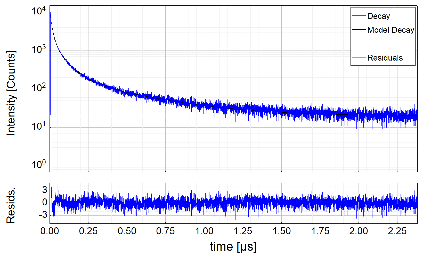
This laboratory houses cutting-edge commercial characterisation tools as well as tools currently being developed by SERIS. It contains a time-resolved photoluminescence tool, which is used to measure the luminescence spectrum of perovskite materials and their effective carrier lifetime, ranging from picoseconds to microseconds. The lab also includes a LED-based modulated PL setup and a high-resolution spectral response system, modified in-house to study the optoelectronic properties of perovskite samples.


Time-resolved fluorescence spectroscopy is a technique used to study various transient events in fluorescent and semiconductor samples, such as charge carrier transfer and recombination, down to sub-nanosecond time resolution. This capability makes it ideal for studying carrier lifetimes in direct-bandgap semiconductors like InGaP, GaAs, InGaN, and perovskites. The setup currently employs two pulsed lasers providing optical excitation at 520 and 760 nm.

Time-resolved photoluminescence (PL) of a perovskite film showing the PL decay, and fitted model decay. The residual trace (bottom panel) indicates good agreement between the fitted and measured data.

Scroll to Top